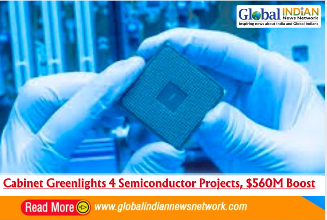
 The Union Cabinet, led by Prime Minister Narendra Modi, has approved four new semiconductor projects under the India Semiconductor Mission (ISM) framework, marking a significant boost to the nation’s semiconductor ecosystem. This decision adds to six previously approved projects currently progressing at various stages.
The new approvals include the country’s first commercial compound semiconductor fabrication facility and an advanced glass-based substrate packaging unit. These projects are expected to support India’s expanding chip design capabilities, which are currently aided by government-backed design infrastructure across 278 academic institutions and 72 startups.
Given the rising demand for semiconductors in sectors such as telecommunications, automotive, data centers, consumer electronics, and industrial electronics, the new projects will play a pivotal role in advancing the Atmanirbhar Bharat initiative focused on self-reliance.
The approved proposals come from SiCSem Private Limited, Continental Device India Private Limited (CDIL), 3D Glass Solutions Inc., and Advanced System in Package (ASIP) Technologies. Collectively, these units represent an investment of around $560 million and are projected to generate employment for 2,034 skilled workers, while also stimulating indirect job creation within the electronics manufacturing ecosystem.
With these additions, the total number of ISM-approved projects reaches ten, involving investments nearing $19.5 billion USD across six states. The new facilities are geographically spread: SiCSem and 3D Glass are based in Info Valley, Bhubaneswar, Odisha; CDIL operates in Punjab; and ASIP is located in Andhra Pradesh.
SiCSem, partnering with UK-based Clas-SiC Wafer Fab Ltd., will develop an integrated Silicon Carbide (SiC) Compound Semiconductor fabrication unit capable of producing 60,000 wafers annually and packaging 96 million units. These components will cater to diverse sectors including defense, missiles, electric vehicles, railways, fast chargers, data centers, consumer appliances, and solar inverters.
3D Glass Solutions Inc. will establish an advanced packaging and embedded glass substrate manufacturing unit in Odisha. Employing cutting-edge technology such as glass interposers, silicon bridges, and 3D Heterogeneous Integration modules, the facility aims to produce 69,600 glass panel substrates, 50 million assembled units, and 13,200 3DHI modules annually. These products are crucial for defense, high-performance computing, AI, automotive, photonics, and optics applications.


